VTAP25 Electrical integration
Power
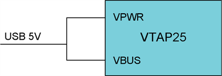
The following power connection scenarios are available
If there is insufficient voltage at start up, for the VTAP board type to be determined, VTAP processes will not start and instead the factory LED will flash at 3 second intervals.
NFC antenna
As the VTAP25 does not have an NFC antenna, an external matched NFC antenna must be connected to the VTAP25 module to use any VTAP functionality. The antenna can be an off‑the‑shelf or a custom antenna depending on the project requirements and level of RF design expertise available.
Your choice of NFC antenna will be affected by the type of enclosure you are designing to house the VTAP25 module and the NFC antenna, the desired user experience, and your approach to radio testing and certification of your end product.
-
Integrate a suitable tuning circuit into your own antenna assembly;
-
Design a separate tuning circuit that can be mounted in between the VTAP25 module and off‑the‑shelf external antenna
Also pay special attention to the type of the NFC antenna, if it is to be mounted very close to a metal surface / LCD screen.
CAUTION: Always ensure sufficient clearance between the NFC antenna and other RF transmitters, to avoid electromagnetic interference between equipment. Clearance required varies between antennas, depending on antenna size, power and sensitivity.
If you have not yet chosen or designed an antenna and matching circuit, Dot Origin can provide support for integrating off‑the‑shelf or custom NFC antennas with the VTAP25 in your device, contact vtap‑support@dotorigin.com.
Filtering
There can be significant radiated emissions where an antenna is connected to the VTAP25 module using a cable that positions the antenna some distance from the ground environment of the VTAP25 module.
Filtering can be very effective in reducing these types of emissions; however, it is not possible to define one solution that will be effective in all scenarios. Any filtering changes the tuning requirements of the matching circuit, and the matching process is made more complicated by the addition of filters. Where space permits and antenna characteristics make it possible to tune the matching circuit with filtering in place, a combined common mode and differential mode filter is recommended to mitigate unwanted emissions. A ground plane extending from the VTAP25 module up to the antenna connector is also recommended.
The following schematics show examples of the different types of filter:
Antenna matching
A matching or tuning circuit ensures that there is optimum power transmitted between the module and the antenna, Tuning is essential to NFC transmission, since imperfect antenna matching or tuning can cause high power loss and poor antenna performance.
Multiple factors can affect the antenna matching, including length of the conductor between the VTAP25 module, matching circuit and the antenna, the size of the antenna and any nearby metal objects. Hence the antenna tuning process should be carried out with the antenna fitted into the final product and mounted in a manner representative of normal use.
Important considerations and examples of tuning circuits suited to specific off-the-shelf antennas are provided in the VTAP Application Note about external antennas.
The VTAP25 has test pads on the bottom of the module for connecting a Vector Network Analyser (VNA) to measure antenna tuning parameters.
See the Reference schematics section for an example NFC antenna circuit. The values of resistors and capacitors are determined during the antenna matching.
These are the main steps involved in antenna matching circuit design and verification:
-
Find the antenna characteristics of your antenna. This is done by finding DC resistance, self‑resonance frequency and inductance of the antenna. These measurements are carried out with the antenna disconnected from the matching circuit. This may involve removing matching circuit components.
-
Calculate the series and parallel capacitor values.
-
Test circuit performance by measuring S11 impedance into the antenna circuits (includes filters, matching circuit and antenna). Use the test pads on the bottom of the module to access these nodes.
Although the VTAP25 uses a later generation of NFC front end chip, it is useful to refer to NXP’s Application Note #AN13219 PN7160 antenna design and matching guide for calculations and further help.
Antenna connection
If the antenna is part of the PCB copper, tracks from the VTAP25 to the antenna should not exceed 100mm per track. The tracks should be routed as close together as possible to minimise loop area.
The antenna matching circuit may be placed near the VTAP25 or near the antenna. It should not be placed at a midpoint.
It is recommended that any circuits are at least 5mm from antenna tracks. If circuits are placed within the antenna area, a ground plane should be used in the component area, but should be kept as far from the antenna wiring as possible. Circuit connections may cross antenna tracks, but crossings should be perpendicular.
CAUTION: Placing connected circuits inside and outside the antenna area, such that tracks cross the antenna, is likely to increase unwanted radiated emissions.
Where the antenna is connected by wires, it is recommended that tracking between the VTAP25 and connection point of wiring should be as short as possible and not exceed 40mm. Wiring should be twisted pair. It is recommended that you avoid bundling antenna connections with other product wiring. Connectors for wiring do not need to be specialised - simple pin header parts will usually suffice. It is recommended that you avoid connectors where the conductors are more than 3mm apart.
FCC/ISED approved NFC antenna
Below are the details of the FCC/ISED approved NFC antenna to use with VTAP25:
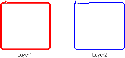
Two-layer PCB trace antenna
Outer dimensions: 40mm x 40mm / 1.57in x 1.57in
Turns: 3
PCB track width: 0.5mm / 0.02in
Gap between tracks: 0.7mm / 0.0275in
Series inductance 0.9936uH (@1MHz)

Layers for VTAP25 reference antenna
The Dot Origin ANT1, ANT4 and ANT6 boards use 40mm x 40mm PCB trace antennas. Please contact us for more information about these.
Use the tuning circuit below with the 40mm x 40mm antenna.

Tuning circuit used with VTAP25 reference antenna
Note: The VTAP25 module is only FCC/ISED approved when used with this antenna. Certification is only valid when the integrator/manufacturer adheres to the trace reference design provided above.
Hardware reset
The VTAP25 does not require an external reset signal. However, it is recommended that pin 27 RESET is connected to a suitable GPIO on the host processor to allow it to force a reset of the VTAP25, should this be necessary. Connect pin 27 RESET to the host and pull low to reset the VTAP25.


