External antenna matching or tuning
A matching or tuning circuit ensures that there is maximum power transmitted between the antenna and the RF transmitter device, with the antenna working only in the desired frequency band (13.56MHz), and minimum signal loss between the transmitter and antenna (return loss/VSWR). Tuning is essential to NFC transmission, since imperfect antenna matching or tuning can cause high power loss and poor antenna performance, and in some cases lead to circuit failure.
Multiple factors such as length of conductor, metal surfaces in close proximity, ferrite sheets, or other emitters within 20cm of the NFC antenna, can also alter the tuning of the antenna. LCD screens or keypads can also affect the tuning of an antenna mounted behind the screen, due to the associated metalwork.
Please consult VTAP support at an early stage, to discuss your plans and resolve any antenna tuning issues. It is always advisable to tune the antenna in the final housing, mounted in a manner representative of normal use, so that all factors are taken into account.
Here are main steps involved in antenna matching circuit design and verification:
-
Find the characteristics for your antenna. This involves measuring DC resistance, self resonant frequency and inductance of the antenna. These measurements are carried out with the antenna disconnected from the matching circuit, which may involve removing matching circuit components.
-
Calculate the series and parallel capacitor values required.
-
Test circuit performance by measuring S11 impedance into the antenna circuits (including filters, matching circuit and antenna). When antenna tuning for VTAP25, use the test pads on the bottom of the module to access these nodes. Equivalent tuning points on VTAP50 are not accessible.
For more detailed information with calculations you may find it useful, refer to NXP Application Note AN13219.
Antenna matching circuit for VTAP50

We have designed matching circuits for various off‑the‑shelf NFC antennas, which could be readily used with the VTAP50 in indoor, office environments. (These tuning circuits are not off‑the‑shelf accessories, only examples of the type of design required. You will need to make design decisions about where best to accommodate the tuning circuit, refer to External antenna choices. You will need to test achieved performance in your actual range of application scenarios and environments, before selecting any of these examples for production.) The example antennas are:
(The ANT-x numbers are Dot Origin identifiers for particular tested antenna, cable and tuning circuit combinations. Refer to Annex A Tested external antennas for a list with any certifications obtained.) Component values provided in the following tables to integrate the example antennas, all relate to the tuning circuit Figure 4-1 above.
Note: If you need matching circuit calculations for another NFC antenna, or other support in custom NFC antenna design, please contact vtap‑support@dotorigin.com with your requirement to explore how we can support you.
Matching circuit examples for off‑the‑shelf antennas
The read ranges mentioned for these example were measured with an NFC Type2 card, and with no metal or transmitters within 30cm. These ranges should be used as a reference point only. Range will vary depending on the environment, enclosure, and the phone or type of card from which the data is being read.
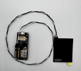
CAUTION: All values are calculated using the standard out-of-the-box cable arrangements (100mm/400mm where mentioned) and a VTAP50‑M2 matching header PCB, as shown in the photographs. If you are designing your own matching board it needs to be designed and mounted on the expansion header in similar fashion. Changes in component values, matching board style or cable length will change the characteristic and result in a mismatch.
There are two sets of matching circuit components for this antenna model:
-
antenna without a cable (standard out-of-the-box arrangement); and
-
antenna with a pair of 24AWG, 100mm long cable.

Matching circuit component values for Figure 4-1.
|
Component |
Value |
Remarks |
|
C1 |
- |
- |
|
C2 |
56pF |
Cseries |
|
C3 |
68pF |
Cshunt |
|
C4 |
- |
- |
|
C5 |
10pF |
Cshunt |
|
C6 |
68pF |
Cshunt |
|
C7 |
10pF |
Cshunt |
|
C8 |
56pF |
Cseries |
|
R1 |
3.3Ω |
Rseries |
|
R2 |
3.3Ω |
Rseries |
This arrangement provides an NFC read range of up to 90mm with a typical NFC/contactless card. The range with other physical cards and tags will depend on their own antenna shape and size, while the operating distance for mobile phones and NFC Wallets/apps will also vary depending on multiple factors including the shape, size and position of the phone’s NFC antenna. Performance is also affected by the presence of metal in the vicinity and the distance between the antenna and the front surface of the chosen enclosure.
Matching circuit component values for Example board schematic for antenna matching or tuning for VTAP50.
|
Component |
Value |
Remarks |
|
C1 |
33pF |
Cseries |
|
C2 |
10pF |
Cseries |
|
C3 |
75pF |
Cshunt |
|
C4 |
33pF |
Cseries |
|
C5 |
- |
- |
|
C6 |
75pF |
Cshunt |
|
C7 |
- |
- |
|
C8 |
10pF |
Cseries |
|
R1 |
2.7Ω |
Rseries |
|
R2 |
2.7Ω |
Rseries |
This arrangement provides an NFC read range of up to 95mm with a typical NFC/contactless card. The range with other physical cards and tags will depend on their own antenna shape and size, while the operating distance for mobile phones and NFC Wallets/apps will also vary depending on multiple factors including the shape, size and position of the phone’s NFC antenna. Performance is also affected by the presence of metal in the vicinity and the distance between the antenna and the front surface of the chosen enclosure.
This antenna comes without a connecting cable. We have calculated the matching circuit for this NFC antenna with a pair of 24AWG, 102mm long cable.

Matching circuit component values for Figure 4-1.
|
Component |
Value |
Remarks |
|
C1 |
68pF |
Cseries |
|
C2 |
- |
- |
|
C3 |
150pF |
Cshunt |
|
C4 |
68pF |
Cseries |
|
C5 |
- |
- |
|
C6 |
150pF |
Cshunt |
|
C7 |
- |
- |
|
C8 |
- |
- |
|
R1 |
1.0Ω |
Rseries |
|
R2 |
1.0Ω |
Rseries |
This arrangement provides an NFC read range of up to 50mm with a typical NFC/contactless card. The range with other physical cards and tags will depend on their own antenna shape and size, while the operating distance for mobile phones and NFC Wallets/apps will also vary depending on multiple factors including the shape, size and position of the phone’s NFC antenna. Performance is also affected by the presence of metal in the vicinity and the distance between the antenna and the front surface of the chosen enclosure.
This 45x55mm antenna comes with a 102mm long, 28AWG cable and a Micro-Lock Plus connector. It has a ferrite sheet on one side and adhesive mounting on the other side.

Matching circuit component values for Figure 4-1.
|
Component |
Value |
Remarks |
|
C1 |
33pF |
Cseries |
|
C2 |
- |
- |
|
C3 |
33pF |
Cshunt |
|
C4 |
33pF |
Cseries |
|
C5 |
4.7pF |
Cshunt |
|
C6 |
33pF |
Cshunt |
|
C7 |
4.7pF |
Cshunt |
|
C8 |
- |
- |
|
R1 |
1.5Ω |
Rseries |
|
R2 |
1.5Ω |
Rseries |
This arrangement provides an NFC read range of up to 75mm with a typical NFC/contactless card. The range with other physical cards and tags will depend on their own antenna shape and size, while the operating distance for mobile phones and NFC Wallets/apps will also vary depending on multiple factors including the shape, size and position of the phone’s NFC antenna. Performance is also affected by the presence of metal in the vicinity and the distance between the antenna and the front surface of the chosen enclosure.
This 34.39x46.1mm antenna comes with a 102mm long, 28AWG cable and a Micro-Lock Plus connector. It has a ferrite sheet on one side and adhesive mounting on the other side.

Matching circuit component values for Figure 4-1.
|
Component |
Value |
Remarks |
|
C1 |
33pF |
Cseries |
|
C2 |
- |
- |
|
C3 |
27pF |
Cshunt |
|
C4 |
33pF |
Cseries |
|
C5 |
- |
- |
|
C6 |
27pF |
Cshunt |
|
C7 |
- |
- |
|
C8 |
- |
- |
|
R1 |
1.5Ω |
Rseries |
|
R2 |
1.5Ω |
Rseries |
This arrangement provides an NFC read range of up to 70mm with a typical NFC/contactless card. The range with other physical cards and tags will depend on their own antenna shape and size, while the operating distance for mobile phones and NFC Wallets/apps will also vary depending on multiple factors including the shape, size and position of the phone’s NFC antenna. Performance is also affected by the presence of metal in the vicinity and the distance between the antenna and the front surface of the chosen enclosure.
This 34.39x46.1mm antenna comes without a cable. We have tuned it with a 400mm long, 28AWG cable and a Micro‑Lock Plus connector. It has a ferrite sheet on one side and adhesive mounting on the other side.
Matching circuit component values for Figure 4-1.
|
Component |
Value |
Remarks |
|
C1 |
33pF |
Cseries |
|
C2 |
- |
- |
|
C3 |
10pF |
Cshunt |
|
C4 |
33pF |
Cseries |
|
C5 |
4.7pF |
Cshunt |
|
C6 |
10pF |
Cshunt |
|
C7 |
4.7pF |
Cshunt |
|
C8 |
- |
- |
|
R1 |
1.5Ω |
Rseries |
|
R2 |
1.5Ω |
Rseries |
This arrangement provides an NFC read range of up to 65mm with a typical NFC/contactless card. The range with other physical cards and tags will depend on their own antenna shape and size, while the operating distance for mobile phones and NFC Wallets/apps will also vary depending on multiple factors including the shape, size and position of the phone’s NFC antenna. Performance is also affected by the presence of metal in the vicinity and the distance between the antenna and the front surface of the chosen enclosure.
This 15x25mm antenna comes with a 102mm long, 28AWG cable and a Micro-Lock Plus connector. It has a ferrite sheet on one side and adhesive mounting on the other side.

Matching circuit component values for Figure 4-1.
|
Component |
Value |
Remarks |
|
C1 |
33pF |
Cseries |
|
C2 |
10pF |
Cseries |
|
C3 |
33pF |
Cshunt |
|
C4 |
33pF |
Cseries |
|
C5 |
4.7pF |
Cshunt |
|
C6 |
33pF |
Cshunt |
|
C7 |
4.7pF |
Cshunt |
|
C8 |
10pF |
Cseries |
|
R1 |
1.5Ω |
Rseries |
|
R2 |
1.5Ω |
Rseries |
This arrangement provides an NFC read range of up to 35mm with a typical NFC/contactless card. The range with other physical cards and tags will depend on their own antenna shape and size, while the operating distance for mobile phones and NFC Wallets/apps will also vary depending on multiple factors including the shape, size and position of the phone’s NFC antenna. Performance is also affected by the presence of metal in the vicinity and the distance between the antenna and the front surface of the chosen enclosure. It is at the lower size/performance limit to support the Apple ECP2/Access minimum 40mm range requirement with all models of iPhone and Apple Watch, depending on the enclosure.
Antenna matching circuit for VTAP25‑MOD
A VTAP25 reader module requires a matching circuit in the same way as VTAP50.

Example board schematic for antenna matching or tuning for VTAP25
Please refer to the
Antenna connection and placement of the tuning circuit is a particular consideration for VTAP25.
If the antenna is part of the PCB copper, tracks from the VTAP25 to the antenna should not exceed 100mm per track. The tracks should be routed as close together as possible to minimise loop area.
The antenna matching circuit may be placed near the VTAP25 or near the antenna. It should not be placed at a midpoint.
It is recommended that any circuits are at least 5mm from antenna tracks. If circuits are placed within the antenna area, a ground plane should be used in the component area, but should be kept as far from the antenna wiring as possible. Circuit connections may cross antenna tracks, but crossings should be perpendicular.
CAUTION: Placing connected circuits inside and outside the antenna area, such that tracks cross the antenna, is likely to increase unwanted radiated emissions.
Where the antenna is connected by wires, it is recommended that tracking between the VTAP25 and connection point of wiring should be as short as possible and not exceed 40mm. Wiring should be twisted pair. It is recommended that you avoid bundling antenna connections with other product wiring. Connectors for wiring do not need to be specialised - simple pin header parts will usually suffice. It is recommended that you avoid connectors where the conductors are more than 3mm apart.
Ferrite shielding of metal surfaces
Metal surfaces nearby can significantly degrade antenna performance by inducing eddy currents that oppose the antenna’s magnetic field, reducing efficiency and read range. Ferrite shielding is a proven and effective method to mitigate these effects and enhance system reliability in 13.56 MHz NFC and RFID systems.
The degree to which metal interferes with antenna operation depends on several factors, including the size and conductivity of the metal, the antenna Q factor, system sensitivity, and target read range. However, as a general rule, if metal is located within approximately 15‑20mm of the antenna coil in any direction, ferrite shielding is strongly recommended. For larger clearances, shielding may not be required, but system‑level testing should always be carried out to confirm that.
Many off-the-shelf antennas, including some mentioned in this document, are supplied with integrated ferrite, but this should be verified before installation. Proper shielding placement and validation are essential to minimise losses from nearby metal and ensure a stable magnetic field.
For systems using the integrated antenna on the VTAP50‑OEM, VTAP100‑OEM or VTAP100‑OEM assemblies, ferrite shielding can be equally helpful if metal is nearby, when applied externally behind or around the VTAP reader. However, since integrated antennas are fixed in layout and tuning, the addition of ferrite requires careful system‑level testing, to ensure it does not detune or degrade the performance of the reader.
Choose the right type of ferrite
Use ferrite sheets specifically rated for operation around 13.56 MHz, with a high magnetic Q factor (meaning high μ′ and low μ″) to minimise energy losses and optimise magnetic coupling, such as Würth ferrite sheet 364 002.
Choose the correct position for ferrite
Ferrite shielding is typically applied directly behind the antenna coil, particularly when mounted on or near metal surfaces, but can also be positioned beside or around the coil where lateral or surrounding metal is present. This guidance applies whether you are designing a new NFC antenna coil for VTAP50‑MOD or VTAP25‑MOD, or adding shielding to the integrated antenna on a reader board such as the VTAP50‑OEM.
Modern ferrite sheets are thin, lightweight, and flexible, adding minimal thickness to the assembly, which can be important for compact or space-constrained installations. The ferrite can be applied directly onto metal surfaces, with the antenna coil mounted directly on the ferrite to maximise magnetic coupling. Avoid introducing any air gap between the antenna and ferrite, as this can degrade shielding effectiveness and detune the system.
We can provide custom antenna design services for VTAP50-MOD and VTAP25-MOD tailored to your application, ensuring the antenna is optimised and tuned for its final environment. For off-the-shelf antennas not listed in this document, we can also offer tuning support to help you achieve reliable system-level performance.
Test effectiveness after shielding
Regardless of antenna type or shielding approach, it is essential to test the performance of the final assembly with a representative sample of devices (phones/watches) and the card/tag types and sizes which will be used in your application. This should confirm that the system meets all operational requirements in real‑world environmental conditions, including shielding effectiveness, optimum power dissipation from the VTAP reader, and read range.
For more information on ferrite shielding, you might want to refer to the following documents from other manufacturers in this field:
• NXP Application Note AN13219 – PN7160 Antenna Design and Matching Guide
• Würth Application Note – Going Wireless with Magnetic Shielding
• Molex Application Note – Design Guide for NFC Antennas and Ferrite Sheet Application