VTAP25 Recommendations for PCB layout
Module dimensions
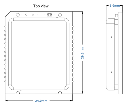
The module dimensions are 24mm x 29.3mm x 5.9mm (0.95in x 1.15in x 0.23in).
Please contact vtap‑support@dotorigin.com for 3D model of the module.
Holes for test pads
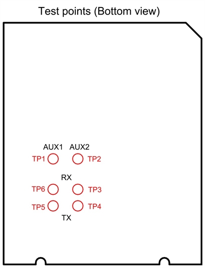
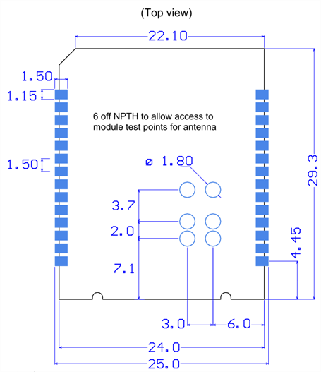
To facilitate user tuning, there are six pads on the bottom of the module. The host board must accommodate for these holes for future accessibility. These pads connect to the antenna drive pins on the NFC controller to allow connecting a VNA for tuning purposes and to the receive pins and test-bus pins for future validation. See the VTAP25 footprint for the test pad dimensions.
Footprint
All dimensions are in mm.
Soldering
Solder the module in a single reflow. Use the lead-free alloy Sn96.5Ag3Cu0.5, also known as the SAC305.
Recommended reflow profile (Standard)
-
Ramp‑up 1‑3°C /sec
-
Pre-heating 150‑180°C, 30‑90sec
-
Heating >220°C, 30‑75sec
-
Peak temperature 240°C ± 3 °C, ≤ 30sec
-
Cooling zone -1 to -5°C /sec
The VTAP25 is rated at the moisture sensitivity level (MSL) of 3. Once the module is unpacked from the sealed ESD protective bags, it must be soldered within 168 hours under the factory conditions 25 ± 5°C and 60 %RH. If not soldered within this time period, the module needs to be baked before soldering.
Follow these instructions for baking, depending on the packaging type (reel/tray).
-
Reel should be baked at 40°C for 192 hours.
-
JEDEC trays can be baked 40°C for 192 hours, or 125°C for 25 hours.


